


Updated on May 29, 2026
A Smart Memories chip is made up of many processing tiles, each containing local memory, local interconnect, and a processor core. For efficient computation under a wide class of possible applications, the memories, the wires, and the computational model can all be altered to match the applications.
To show the applicability of this design, two very different machines at opposite ends of the architectural spectrum, the Imagine stream processor and the Hydra speculative multiprocessor, are mapped onto the Smart Memories computing substrate. Simulations of the mappings show that the Smart Memories architecture can successfully map these architectures with only modest performance degradation.
The memory system is of growing importance in processor design. Different applications have different memory access patterns and thus require different memory configurations to optimize performance. Often these different memory structures require different control logic and status bits. Therefore, a memory system that can be configured to closely match the application demands is desirable. A recent study of SRAM design shows that the optimal block size for building large SRAMs is small, around a few KB. Large SRAMs are then made up of many of these smaller SRAM blocks. We leverage this naturally hierarchical design to provide low overhead re-configurability. The basic memory mat size of 8KB is chosen based on a study of decoder and I/O overheads and an architectural study of the smallest memory granularity needed.
Allocating a third of the tile area to memory allows for 16 independent 8KB memory mats, a total of 128KB per tile. Each mat is a 1024x64b logical memory array that can perform reads, writes, compares, and read-modify-writes. All operations are bytemaskable. In addition to the memory array, there is configurable logic in the address and data paths. In the address path, the mats take in a 10-bit address and a 4-bit opcode to determine what operation is to be performed. The opcode is decoded using a reconfigurable logic block that is set up during the hardware configuration. The memory address decoder can use the address input directly or can be set in auto-increment/decrement streaming mode.
In this mode, the mat stores the starting index, stream count, and stride. On each streaming mode request, the mat accesses the next word of the stream until reaching the end of the stream. In the data path, each 64-bit word is associated with a valid bit and a 4-bit configurable control field. These bits can be used for storing data state such as cache LRU or coherence bits. They are dual ported to allow read-modify-write operations each cycle and can be flash cleared via special opcodes. Each mat has a write buffer to support pipelined writes and to enable conditional write operations ( e.g. in the case of a cache write). Mats also contain logic in the output read path for comparisons, so they can be used as cache tag memory.
To connect the different memory mats to the desired processor or quad interface port, the tile contains a dynamically routed crossbar, which supports up to 8 concurrent references. The processor and quad interface generate requests for data, and the quad interface and memories service those requests. The crossbar does not interconnect different units of the same type (e.g. memory mat to memory mat communication is not supported in the crossbar). Requests through the crossbar contain a tag indicating the desired destination port and an index into the memory or unit attached to that port. The crossbar protocol always returns data back to the requestor, so data replies can be scheduled at the time of routing the forward-going request. Requests can be broadcast to multiple mats via wildcards, but only one data reply is allowed. The requests and replies are all pipelined, allowing a requestor to issue a new request every cycle. Arbitration is performed among the processor and quad interface ports since multiple requests for the same mat or quad interface port may occur. No arbitration is necessary on the return crossbar routes, since they are simply delayed versions of the forward crossbar routes. From circuit-level models of the crossbar and the memories, the estimated latency for a memory request is 2 processor clock cycles
About half of the time is spent in the crossbar, and the other half is spent in the memory mat. We project that our processor core will have a clock cycle of 20 fanout-of-four inverter delays (FO4s), which is comparable to moderately aggressive current processor designs. In a commodity 0.1mm process, a 20 FO4 cycle time is equivalent to a 1GHz operating frequency. The quad interconnection network, shown in Figure 5, connects the four tiles in a quad together. The network consists of 9 64-bit multicast buses on which any of the 4 tiles or the global network can send or receive data. These buses may also be configured as halfword buses. In addition to these buses, a small number of control bits are broadcast to update state, atomically stall the processors, and arbitrate for the buses. The quad interface on each tile connects the internal tile crossbar to the quad network, thus mediating all communication to and from the tile
The processor portion of a Smart Memories tile is a 64-bit processing engine with reconfigurable instruction format/decode. The computation resources of the tile consist of two integer clusters and one floating-point (FP) cluster. The arrangement of these units and the FP cluster unit mix.
Each integer cluster consists of an ALU, register file, and load/store unit. This arithmetic unit mix reflects a trade-off between the resources needed for a wide range of applications and the area constraints of the Smart Memories tile. Like current media processors, all 64-bit FP arithmetic units can also perform the corresponding integer operations and all but the divide/sqrt unit performs subword arithmetic. The high operand bandwidth needed in the FP cluster to sustain parallel issue of operations to all functional units is provided by local register files (LRFs) directly feeding the functional units and a shared register file with two read and one write ports
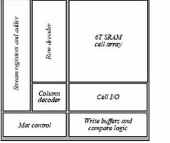
For complex memory structures that need multiple accesses to the same data ( e.g. snooping on the cache tags in a multiprocessor), four of the mats are fully dual-ported. Many applications and architectures also need fully associative memories, which are inefficient and difficult to emulate using mats. Therefore, the tile memory system also contains a 64-entry content-addressable memory ( CAM ). The Smart Memories mats can be configured to implement a wide variety of caches, from simple, single-ported, direct-mapped structures to set-associative, multi-banked designs.
| Are you interested in this topic.Then mail to us immediately to get the full report.
email :- contactv2@gmail.com |
