


Updated on May 29, 2026
As a concept, "System in Package" or "SiP" relates to the objective of merging many or all of the electronic requirements of a functional system or a subsystem into one package. It is a concept that can at once be understood by people familiar with electronics and packaging yet is very difficult to define in absolute terms. The following attributes are used to define SiPs:
• Includes chip-level interconnect technology. In other words flip chip, wire bond, TAB, or other interconnects directly to an IC chip. This distinguishes small SMT board assemblies from being considered SiPs.
• More often than not, the SiP is small in physical size.
• Quite often includes passive components. The passives can be either surface mounted discrete components or can be embedded into or manufactured on the substrate material.
• Typically includes more than one IC chip.
• ?May include other components necessary to bring the SiP to a more complete functional system or subsystem level - such as housings, lids, RF shields, connectors, antennas, batteries, etc.
Quite often the term System-in-Package is used to describe multi-chip IC packages such as stacked die CSPs or MCM-PBGAs. The real power of SiP technology lies in its ability to integrate not only multiple ICs but also other components such as passives, connectors, antennas and so on into the package in order to create fully functional subsystems. System in Package has a parallel in the often-discussed System on Chip (SoC) methodology. While SoC has many good attributes, and has been the focus of several IC manufacturers for several years, by its very nature it is limited by what can be achieved within one wafer process.
It is quite easy to understand that SoC may be limited in the type of IC functions that one would like to design into a system - or at best performance will likely be compromised due to a common wafer process. SiP is not limited by the constraint of a common wafer process, so that IC chips, each optimally suited for its function by both design and wafer fab process, can be easily combined together in one package.
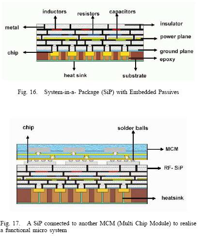
Another SiP solution with Integrated Module Board packaging and assembly technology, which is a variety of SiP with 3-d packaging and assembly technology where individual modules are packaged and assembled as shown in Fig.15. In this case the package has higher reliability, interconnection density and yield. Since every chip is embedded in the core insertion (epoxy), which allows three dimensional volume of the module can be used for component assembly. The manufacturing process is lead free and totally solder less process.
| Are you interested in this topic.Then mail to us immediately to get the full report.
email :- contactv2@gmail.com |
