


Published on Apr 02, 2024
A transistor is a semiconductor device used to amplify or switch electronic signals and electrical power. It is composed of semiconductor material with at least three terminals for connection to an external circuit. A voltage or current applied to one pair of the transistor's terminals changes the current through another pair of terminals. Because the controlled (output) power can be higher than the controlling (input) power, a transistor can amplify a signal.
To Study the Static Characteristic of a Transistor (Common Emitter Configuration)
Bipolar Junction Transistors are transistors which are made up of 3 regions, the base, the collector, and the emitter. A small current entering in the base region of the transistor causes a much larger current flow from the emitter to the collector region. Bipolar junction transistors come in two main types, npn and pnp. A npn transistor is one in which the majority current carrier are electrons. Electron flowing from the emitter to the collector forms the base of the majority of current flow through the transistor. The other type of charge,holes, are a minority. pnp transistors are the opposite. In pnp transistors, the majority current carriers are holes.
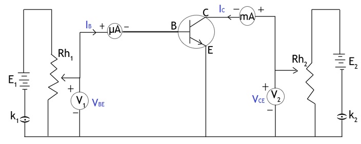
The circuit diagram for npn transistor is shown below.
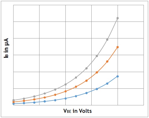
Keeping the collector- emitter (VCE) voltage constant, the base- emitter (VBE) voltage is increased from 0 and the corresponding base current (IB) values are noted. This is repeated for increasing values of VCE. The family of curve obtained by plotting IB against VBE for each VCE value is called input characteristics.
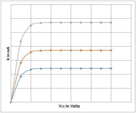
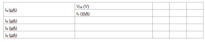
By keeping the base current (IB) constant, collector- emitter (VCE) voltage is varied and the corresponding IC values are obtained. This is repeated for increasing values of IB. The family of curves obtained by plotting IC against VCE for each value of IB is called output characteristics.
Students understand the following terms:
• Transistor
• pnp and npn transistors
• Transistor characteristics
Students will be able to do the experiment, once they understand the procedure.
• Rheostat
• Voltmeter
• Ammeter
• Battery
• One way key
• Transistor
• Bread board
• Connections are made as shown in the circuit diagram.
• The rheostat Rh1 is used to vary base voltage (input voltage) VBE and it is read from voltmeter V1. The base current (input current) IB is measured using a microammeter (µA). The collector voltage (output voltage) VCE is varied using the rheostat Rh2 and readings are noted from voltmeter V2. The collector current (output current) IC is measured by the milliammeter (mA).

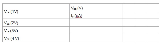
• The collector voltage VCE is kept constant (eg. 1V) by adjusting the rheostat Rh2.
• The base voltage VBE is varied from zero by adjusting the rheostat Rh1.
• The base current IB is noted in each step.
• A graph is drawn with VBE along X-axis and IB along Y-axis.
• The experiment is repeated with VCE kept constant say 2V, 3V, 4V etc. and corresponding graphs are plotted.
• The base current IB is kept constant (eg. 20µA) by adjusting the rheostat Rh1.
• Now the collector voltage is increased by adjusting the rheostat Rh2.
• The corresponding collector current IC is noted.
• A graph is drawn with VCE along X-axis and IC along Y-axis.
• The experiment is repeated with keeping IB constant, say 40µA, 60µA, 80µA etc and similar graphs are plotted.
The graphs shows the input and output characteristics of a transistor.
• http://epathshala.nic.in/wp-content/doc/book/flipbook/Class%20XII/12090-Physics%20Part-II/Chapter%2014/index.html
