


Published on Nov 30, 2023
The design of silicon chips in every semiconductor industry involves the testing of these chips with other components on the board. The platform developed acts as power on vehicle for the silicon chips. This Printed Circuit Board design that serves as a validation platform is foundational to the semiconductor industry. The manual/repetitive design activities that accompany the development of this board must be minimized to achieve high quality, improve design efficiency, and eliminate human-errors. One of the time consuming tasks in the board design is the Trace Length matching. The paper aims to reduce the length matching time by automating it using SKILL scripts.
Keywords: — Trace length calculation, Board design, SKILL script, python script
The design of the Printed Circuit Board (PCB) can be done using any of the CAD tools. Computer-aided design (CAD) can be defined as the use of computer systems to assist in the creation, modification and analysis or optimization of a design. (Computer Aided Design and Manufacturing, K.Lalit et al., 2008) PCB Designer speeds designs from placement through routing till manufacturing with powerful features such as partitioning of design, RF design capabilities, and interconnection of design planning. This PCB design solution is highly scalable and production-proven to increase productivity and help the users to quickly ramp up to volume production. SKILL is the scripting language used to build its ECAD tools.
Before defining the problem of trace length calculation, understanding the board terms is important.
A. Abbreviations and Acronyms
Schematics for electronic circuits are designed by design engineers using EDA (electronic design automation) tools called as schematic capture tools. They are drawn as a series of lines and symbols representing the circuit. (Engineering Drawing and Design, David.A et al.) These apparatuses go past straightforward drawing of devices and associations. They are integrated into the IC design flow for validation and simulation of the circuit.
Each of the elements on the Schematic design is associated with a part number. The schematics use logical part numbers while the physical part numbers specific to organizations are different.
An electronic symbol is a pictogram used to symbolize electrical and electronic devices like wires, resistors, batteries and transistors in a schematic diagram of a circuit. These symbols can vary between countries but are mostly standardized internationally.
A footprint or a pattern is the arrangement of pads (in surface-mount technology) or throughholes (in through-hole technology) used to electrically connect and physically attach components to PCB. The pattern on a circuit board matches the arrangement of leads on a component
A central database that stores all the symbol and footprints of different boards
CAD tool’s file format for Schematic parts • Net: A net is a conductor that interconnects 2 or more component terminals
The length of the connection on external layers of the circuit is called microstrip while the length in between the layers is called stripline length
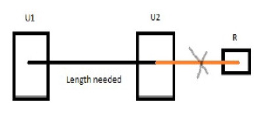
When a board design is in process, there are rules that need to be followed. One of the rules is that the total length of high speed signal routings must not exceed a threshold value. The micro strip and the strip line lengths must be extracted separately from the board to verify the lengths. When a connection is made from a component U1 to component U2, the connection ends with a resistor. This length is called as termination length or the dangling length.
To calculate lengths, the CAD tool provides in built reports which are drawn for a given board. There is a layer by layer length report that can be extracted from this tool. This provides the length of each connection on multiple layers. The total length of a connection and the dangling lengths must be manually extracted from the report. The board design will be followed by the board tape out. At each stage of the design, it must be checked for its correctness. This means that the length reports from the CAD tool must be extracted and the manual calculations must be done each time there is a change in the board. This is a tedious task and consumes precious time during board tape outs.
The solution to this problem is the development of a SKILL script that calculates the distance between 2 components for all the nets in the board. The SKILL script starts the length calculation from point1 and stops when point2 is reached. This eliminates the inclusion of the dangling length. It also separately calculates the length of the net as microstrip and stripline. The execution of this script produces a text report that contains the net names, total lengths, micro strip and strip line lengths. The script also provides the break point in the net if there exists any in the case of a T junction. It provides separate lengths to each end point from the breakpoint observed. This will help to calculate the dangling length but does not include it in the total length calculation.
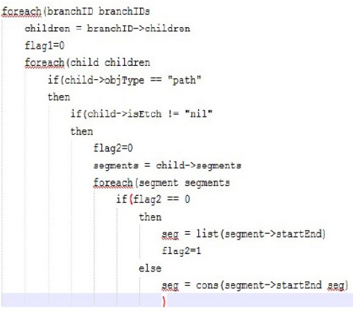
In electronic design, a netlist is a description of the connectivity of an electronic circuit. A single netlist is a collection of several related lists. A much simpler definition states that a netlist consists of a list of the terminals (pins) of the electronic components in a circuit and a list of the electrical conductors that interconnect the terminals. A net is a conductor that interconnects two or more component terminals. Branches are edges of a circuit. Each branch has children. Children can be “paths”, “vias” or “pins”. A path consists of line segments or arc segments.
The below code snippet traverses the entire path, from Net Name till the segments. It obtains the start and end points of the segments.
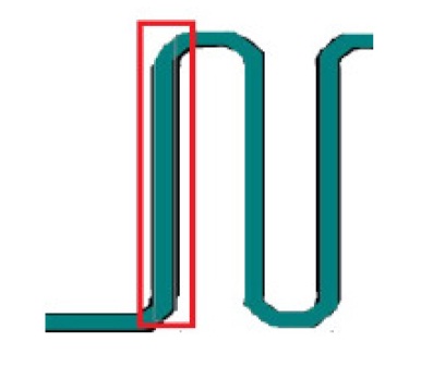
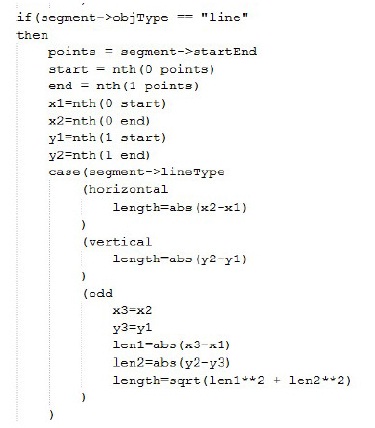
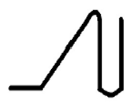
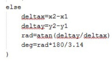
The line segments can be horizontal or vertical or odd as shown in the figure below. The length of horizontal and vertical segments can be calculated by subtracting the x and y locations of the end points. However the odd line length must be calculated using Pythagoras theorem.
The below code snippet shows the implementation of the line types.
The length of the line segments can be easily calculate d. These segments might also contain arcs whose length might be crucial.
The arc length must be calculated separately as shown below in the code snippet.
The SKILL code is saved with a .il extension. The code can be loaded on the PCB Editor using the command: Load(“TLC.il”) Once the script is loaded, the function name must be called to execute the script.
The function accepts inputs of component 1 and 2. The Netlist file can also be provided as an input. In this solution, the netlist name and location are hardcoded in the program.The output file is created in the same location where the script and the input files are stored. The output file consists of the lengths as below.

The SKILL script developed helps calculate the lengths in minutes which earlier was taking more than 1 working day. The script works significantly if the board design is accurate. It also works if the board contains vias that are misplaced at the terminating end of the connection. However, if the board contains vias that are misplaced at the connection beginning, the SKILL script fails to extract the net length as it does not find the right pin in the beginning. The way to find out the misplaced via and its length extraction when the board is not accurate is the future work of this script.
[1] Engineering Drawing and Design by David.A. Madsen, David.P.Madsen, 2012, P 811
[2] Computer Aided Design and Manufacturing by K.Lalit Narayan, K.Mallikarjun Rao, M.M.M.Sarcar
[3] http://www.intel.com
[4] http://library.intel.com
