


Published on Apr 02, 2024
This activity is designed for high school students. In this experiment students use light to transfer a pattern onto a surface, either a network of very small metal wires or self-drawn patterns on a plastic board. The pattern is transferred by placing a mask (transparency sheet with the pattern) on a plastic board. The board is coated with a copper film that is covered with a light-reactive polymer (photo-resist). The polymer is exposed to UV light through the mask to make a pattern in the polymer. The metal under the exposed polymer is then chemically etched, leaving only the pattern on the surface of the board as determined by the mask. This top-down approach to nanotechnology is commonly used in manufacturing circuit boards for computers and other electronics.
Demonstrate the top-down approach to fabrication of nanometer sized electronic components commonly used in manufacturing circuit boards for computers and other electronics and teach the basic chemistry and physics necessary for photolithography.
As a result of participating in this program, students will be able to:
1. Understand what lithography is and become familiar with different types of lithography.
2. Get a conceptual understanding of photolithography, and understand the Physics and Chemistry behind it.
3. Draw a simple pattern for a mask, and transfer it onto a plastic board covered with copper and a thin film of photo resist.
4. Etch the unwanted copper away to result in the pattern in copper.
• UV exposure station, consisting of 2 UV lamps (black lights)
• Black cloth or big basket to cover the UV lamps.
• Applicator sticks of Photoresist Stripper
• Large Beakers (plastic and glass, 500 to 750 ml)
• Small Beakers (150-250ml)
• Glass Slides
• Tweezers
• Photomasks (electrode pattern on transparency)
• Permanent Marker
• 250 mL Glass Beakers
• Watch Glass (Beaker Cover)
• Heat resistant gloves
• Stopwatch timer
• Digital Multimeter
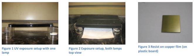
Keep room lights to a minimum until after developing is done. Exposure: Take a piece of prepared circuit board that has black tape covering the top side. The tape protects the underlying photoresist layer from light. Have each student write its name or initials on the back of the circuit board with the supplied marker. Give each one a preprinted mask and/or a marker for drawing their pattern. Have your UV exposure station (UV light off) completely ready (see Figure 1 and 2 for setup guidelines). Cover the setup with black cloth covering most of the lamp with enough space to slide in all the boards.
Let each student bring their circuit board+mask to you, just before place it under the UV light, peel off the black tape to reveal the photoresist. Be careful not to get fingerprints on the photoresist. This should be done at the last minute to avoid exposing the photo-resist to the ambient light. Make sure the black pattern of the mask is completely on the substrate. Be careful not to put fingerprints on the mask and that all the circuit boards are positioned directly under one of the bulbs of the UV lamps.
a. Place a clean glass slide on top of the mask, to keep the mask flat against the photoresist. Again, be careful to avoid getting any fingerprints or dust on the glass slide. Photomasks being placed unevenly will result in blurry patterns and inconsistent developing and etching.
b. Cover the black cloth over the entire setup. Take care not to knock over the UV lights. Ensure that the covering is such that the room lights are not interfering with the exposure.
c. Use a timer to expose the boards for 12 min. Do not over expose.
a. Pour the developer solution into the small glass/plastic beaker and fill large plastic beakers with water. Label the two beakers, developer solution and rising water.
b. Two substrates can be developed in each developer beaker simultaneously. Place them back to back such that the exposed surfaces both face outwards (use a pair of locking tweezers to do so). Try not to touch the pattern left by the photomask
c. Gently shake/stir with the tweezers for 40 seconds. Use the included stopwatch for accurate timing.
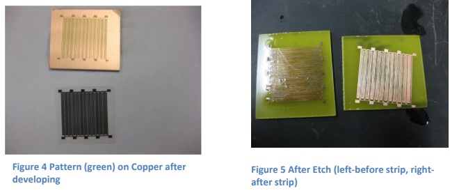
d. Immediately rinse the substrates in the large beaker filled with water to reveal the copper layer with the photomask pattern clearly visible in green and the surrounding copper metal is exposed (see figure 4). Thus, developing removes the photoresist that was exposed to UV light. Development is not complete until you see the pattern from the photomask as a green pattern on top of the copper metal (you can always develop more but cannot go back!). Clean with water after developing is done. e. Now room lights can be turned on fully
a. Once the boards have been developed (i.e. the photoresist has been removed from the unwanted copper), it is time to etch away the unwanted copper so that only the pattern is left.
b. Before starting the etching, check to make sure that the etchant solution is boiling on the hotplate, has a few boiling stones in it and is maintained at or above 80⁰C. (If are planning on leaving it on the hotplate for sometime, cover with a watch glass so that the etchant does not boil away)
c. Use a pair of heat resistant locking tweezers to hold the board. Make sure that the tweezers are not on the pattern needed.
d. Completely immerse the substrates in the boiling etchant solution and gently shake/stir with the tweezers for 40 seconds. Use the included stopwatch for accurate timing. You may wish to wear the heat-resistant gloves during this step. Students can take turns in doing this if you have enough stations.
e. Immediately rinse the substrates in water. Inspect the copper pattern. If the copper around the pattern is still visible, put the substrates in the etchant for an additional 10 seconds, followed by an immediate rinse in water. Continue etching in 10 second intervals until the copper around the circuit pattern is gone, revealing the plastic underneath. Be careful not to over etch, the copper underneath the photoresist covered pattern should not get etched away (see figure 5, left image).
f. After everyone is done etching, turn off the hotplate and let the etchant cool before disposing off or transferring into bottles for reuse.
a. Check the stripper applicator sponge. If it looks dirty, clean it with a damp paper towel. Gently dab the applicator on a paper towel to moisten the sponge with stripper fluid. It may help to squeeze the applicator stick while dabbing.
b. Using the stripper applicator stick, cover the entire photoresist surface, including the edges with stripper solution. The developer will dissolve the photoresist that is covering the copper pattern.
c. Rinse in a beaker with clean water.
d. The copper pattern should appear shiny and metallic (figure 5, right image). If not, repeat the photoresist stripping until all of the photoresist is removed. Dry the board.
1. Limitations of Photo-lithography (in terms of size): The biggest limitation to Photolithography is the wavelength of light. In order to make features smaller than the wavelength of UV (350nm), either a series of lenses or electron beam (e-beam) lithography is used.
2. Sources of error during the experiment: All steps have to be performed very carefully; each step from exposure to etching can cause errors if over/under done.
3. Necessity of clean room facilities, equipment and gear: dust particles are larger than the features being made.
4. Advantages and disadvantages of scaling down size: Speed and space occupied are the biggest advantages to miniaturization; however when the size is scaled down the resistance and heat loss in device also change. If you have the time, you can go into a discussion of Ohm’s law and how resistance varies with size.
Pour the etchant solution into the plastic-ware container. If two beakers were used, both will fit into the container. Make sure the etchant has cooled down sufficiently before pouring into the plastic-ware. Add the neutralizing powder to the solution while mixing. The solution will bubble and begin to rise. Be careful not to let it overflow. Stirring with the supplied spoon will help. Add the quick cement to the solution while stirring. Over time the solution will harden after which it can be thrown into trash. Alternatively you can give it to a local Chemistry lab who disposes chemicals regularly.
Today Nanotechnology is used in the chip industry on a daily basis. Two different approaches are used in the nano manufacturing industry. The first “bottom up” method builds a structure atom by atom or molecule by molecule, much like building a wall by stacking bricks. The second “top down” method involves cutting down a bulk material to the appropriate size, much as a sculptor would carve a statue out of a large block of marble. This top-down approach to nanotechnology is commonly used in manufacturing circuit boards for computers and other electronics.
Though because of the small feature size in the chip industry ( a few nanometers), light cannot be used and they rely on electron-beam lithography, in this experiment, the students will be exposed to its bigger counterpart: photo-lithography. The reason is photo-lithography cannot be used to make features smaller than the wavelength of light (with the smallest being UV around 350nm). For smaller features, x-rays (or e- beams) have to be used.
In this experiment students use light to transfer a pattern onto a surface (either resulting in a network of very small metal wires on a plastic board or any self- drawn pattern) using a top down process. The pattern is transferred by placing a mask with the wanted design on a plastic board. The board is coated with a copper film that is covered with a light-reactive polymer (photo-resist). The circuit boards used here come with a ready-made layer of hardened photoresist under the black tape. The polymer is exposed to UV light through the mask to make a pattern in the polymer. The metal under the exposed polymer is then chemically etched, leaving only the pattern on the surface of the board as determined by the mask.
[1] X-ray Structure Determination A Practical Guide, 2nd edition, George H. Stout and Lyle H. Jensen, John Wiliey & Sons, New York, 1989.
[2] Fundamentals of Analytical Chemistry, 3rd. edition, Saunders Golden Sunburst Series, Holt, Rinehart and Winston, Philadelphia, 1976.
[3] Chemistry and Crystal Growth, Hulliger, J. Angew. Chem. Int. Ed. Engl. (1994) 33, 143-162.
