


Updated on May 29, 2026
The explosion of flash memory technology has dramatically increased storage capacity and decreased the cost of non-volatile semiconductor memory. The technology has fueled the proliferation of USB flash drives and is now poised to replace magnetic hard disks in some applications.
A solid state drive (SSD) is a non-volatile memory system that emulates a magnetic hard disk drive (HDD). SSDs do not contain any moving parts, however, and depend on flash memory chips to store data. With proper design, an SSD is able to provide high data transfer rates, low access time, improved tolerance to shock and vibration, and reduced power consumption. For some applications, the improved performance and durability outweigh the higher cost of an SSD relative to an HDD.
Using flash memory as a hard disk replacement is not without challenges. The nano-scale of the memory cell is pushing the limits of semiconductor physics. Extremely thin insulating glass layers are necessary for proper operation of the memory cells. These layers are subjected to stressful temperatures and voltages, and their insulating properties deteriorate over time. Quite simply, flash memory can wear out. Fortunately, the wear-out physics are well understood and data management strategies are used to compensate for the limited lifetime of flash memory.
Flash memory was invented by Dr. Fujio Masuoka while working for Toshiba in 1984. The name "flash" was suggested because the process of erasing the memory contents reminded him of the flash of a camera. Flash memory chips store data in a large array of floating gate metal–oxide–semiconductor (MOS) transistors. Silicon wafers are manufactured with microscopic transistor dimension, now approaching 40 nanometers.
Intel Corporation introduces its highly anticipated third-generation solid-state drive (SSD) the Intel Solid-State Drive 320 Series. Based on its industry-leading 25-nanometer (nm) NAND flash memory, the Intel SSD 320 replaces and builds on its high-performing Intel X25-M SATA SSD. Delivering more performance and uniquely architected reliability features, the new Intel SSD 320 offers new higher capacity models, while taking advantage of cost benefits from its 25nm process with an up to 30 percent price reduction over its current generation.
SSDs mainly depend on flash memory chips to store data. The name "flash" was suggested because the process of erasing the memory contents reminded him of the flash of a camera. Flash memory chips store data in a large array of floating gate metal–oxide–semiconductor (MOS) transistors. Silicon wafers are manufactured with microscopic transistor dimension, now approaching 40 nanometers. In this flash memory thin insulating glass layers are necessary for proper operation of the memory cells. These layers are subjected to stressful temperatures and voltages, and their insulating properties deteriorate over time. Quite simply, flash memory can wear out.
A floating gate memory cell is a type of metal-oxide-semiconductor field-effect transistor (MOSFET). Silicon forms the base layer, or substrate, of the transistor array. Areas of the silicon are masked off and infused with different types of impurities in a process called doping. Impurities are carefully added to adjust the electrical properties of the silicon.
Some impurities, for example phosphorous, create an excess of electrons in the silicon lattice. Other impurities, for example boron, create an absence of electrons in the lattice. The impurity levels and the proximity of the doped regions are set out in a lithographic manufacturing process. In addition to doped silicon regions, layers of insulating silicon dioxide glass (SiO2) and conducting layers of polycrystalline silicon and aluminum are deposited to complete the MOSFET structure.
MOS transistors work by forming an electrically conductive channel between the source and drain terminals. When a voltage is applied to the control gate, an electric field causes a thin negatively charged channel to form at the boundary of the SiO2 and between the source and drain regions. When the N-channel is present, electricity is easily conducted from the source to the drain terminals. When the control voltage is removed, the N-channel disappears and no conduction takes place. The MOSFET operates like a switch, either in the on or off state.
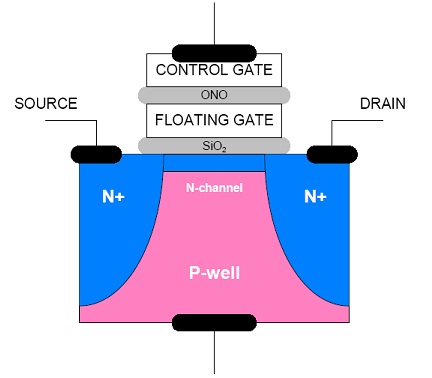
In addition to the control gate, there is a secondary floating gate which is not electrically connected to the rest of the transistor. The voltage at the control gate required for N-channel formation can be changed by modifying the charge stored on the floating gate. Even though there is no electrical connection to the floating gate, electric charge can be put in to and taken off of the floating gate.
A quantum physical process called Fowler-Nordheim tunneling coaxes electrons through the insulation between the floating gate and the P-well. When electric charge is removed from the floating gate, the cell is considered in an erased state.
When electric charge is added to the floating gate, the cell is considered in the programmed state. A charge that has been added to the floating gate will remain for a long period of time. It is this process of adding, removing and storing electric charge on the floating gate that turns the MOSFET into a memory cell.
Erasing the contents of a memory cell is done by placing a high voltage on the silicon substrate while holding the control gate at zero. The electrons stored in the floating gate tunnel through the oxide barrier into the positive substrate. Thousands of memory cells are etched onto a common section of the substrate, forming a single block of memory. All of the memory cells in the block are simultaneously erased when the substrate is “flashed” to a positive voltage. An erased memory cell will allow N-channel formation at a low control gate voltage because all of the charge in the floating gate has been removed. This is referred to as logic level “1” in a single-level cell (SLC) flash memory cell.
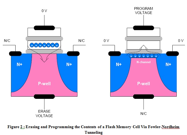
The cell is programmed by placing a high voltage on the control gate while holding the source and drain regions at zero. The high electric field causes the N-channel to form and allows electrons to tunnel through the oxide barrier into the floating gate. Programming the memory cells is performed one word at a time and usually an entire page is programmed in a single operation. A programmed memory cell inhibits the control gate from forming an N-channel at normal voltages because of the negative charge stored on the floating gate. To form the N-channel in the substrate, the control gate voltage must be raised to a higher level. This is referred to as logic level “0” in an SLC flash memory cell.
https://www.intel.com/pressroom/.html
https://www.intel.com/go/ssd/.html
https://www.physorg.com/news/.html
https://www.storageview.com/.html
www. ieeexplore.ieee.org
| Are you interested in this topic.Then mail to us immediately to get the full report.
email :- contactv2@gmail.com |
