


Updated on May 29, 2026
There is a saying in real estate; when land get expensive, multi-storied buildings are the alternative solution. We have a similar situation in the chip industry. For the past thirty years, chip designers have considered whether building integrated circuits multiple layers might create cheaper, more powerful chips.
Performance of deep-sub micrometer very large scale integrated (VLSI) circuits is being increasingly dominated by the interconnects due to increasing wire pitch and increasing die size. Additionally, heterogeneous integration of different technologies on one single chip is becoming increasingly desirable, for which planar (2-D) ICs may not be suitable.
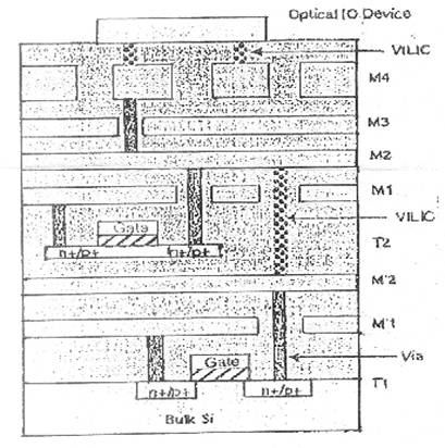
The three dimensional (3-D) chip design strategy exploits the vertical dimension to alleviate the interconnect related problems and to facilitate heterogeneous integration of technologies to realize system on a chip (SoC) design. By simply dividing a planar chip into separate blocks, each occupying a separate physical level interconnected by short and vertical interlayer interconnects (VILICs), significant improvement in performance and reduction in wire-limited chip area can be achieved.In the 3-Ddesign architecture, an entire chip is divided into a number of blocks, and each block is placed on a separate layer of Si that are stacked on top of each other.
The unprecedented growth of the computer and the information technology industry is demanding Very Large Scale Integrated ( VLSI ) circuits with increasing functionality and performance at minimum cost and power dissipation. Continuous scaling of VLSI circuits is reducing gate delays but rapidly increasing interconnect delays. A significant fraction of the total power consumption can be due to the wiring network used for clock distribution, which is usually realized using long global wires.
Furthermore, increasing drive for the integration of disparate signals (digital, analog, RF) and technologies (SOI, SiGe, GaAs, and so on) is introducing various SoC design concepts, for which existing planner (2-D) IC design may not be suitable.
Three-dimensional integration to create multilayer Si ICs is a concept that can significantly improve interconnect performance ,increase transistor packing density, and reduce chip area and power dissipation. Additionally 3D ICs can be very effective large scale on chip integration of different systems.
In 3D design architecture, and entire(2D) chips is divided into a number of blocks is placed on separate layer of Si that are stacked on top of each other. Each Si layer in the 3D structure can have multiple layer of interconnects(VILICs) and common global interconnects.
The 3D architecture offers extra flexibility in system design, placement and routing. For instance, logic gates on a critical path can be placed very close to each other using multiple active layers. This would result in a significant reduction in RC delay and can greatly enhance the performance of logical circuits.
• The 3D chip design technology can be exploited to build SoCs by placing circuits with different voltage and performance requirements in different layers.
• The 3D integration can reduce the wiring ,thereby reducing the capacitance, power dissipation and chip area and therefore improve chip performance.
• Additionally the digital and analog components in the mixed-signal systems can be placed on different Si layers thereby achieving better noise performance due to lower electromagnetic interference between such circuits blocks.
• From an integration point of view, mixed-technology assimilation could be made less complex and more cost effective by fabricating such technologies on separate substrates followed by physical bonding.
A 3D solution at first glance seems an obvious answer to the interconnect delay problem. Since chip size directly affects the inter connect delay, therefore by creating a second active layer, the total chip footprint can be reduced, thus shortening critical inter connects and reducing their delay. However, in today’s microprocessor, the chip size is not just limited by the cell size ,but also by how much meta is required to connect the cells.
The transistors on the Si surface are not actually packed to maximum density, but are spaced apart to allow metal lines above to connect one transistor or one cell to another .The meal required on a chip for inter connections is determined not only by the number of gates ,but also by other factors such as architecture, average fan-out, number of I/O connections, routing complexity, etc Therefore, it is not obvious that using a 3D structure the chip size will be reduced.
| Are you interested in this topic.Then mail to us immediately to get the full report.
email :- contactv2@gmail.com |
