


Published on Apr 02, 2024
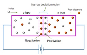
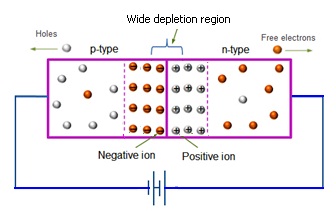
Semiconductor diode is simply the combination of a p-type and an n-type material. It is formed by doping half of the silicon crystal with trivalent impurity (p-type) and the other half with pentavalent impurity (n-type). It has the characteristics of passing current in one direction only. If there is no voltage is applied across the junction, electrons will diffuse through the junction to p - side and holes will diffuse through the junction to n - side and they combine with each other. Thus the acceptor atom near the p - side and donor atom near n – side are left unutilized and is called the depletion layer. An electron field is generated by these uncovered charges which called the barrier potential. This opposes further diffusion of carriers and is known as depletion region
To draw the I-V characteristic curve of a p-n junction diode in forward bias and reverse bias.
Semiconductors are materials with electrical conductivity intermediate between that of a conductor and an insulator. In semiconducting materials thermal energy is enough to cause a number of electrons to release from valance band to conduction band, in which they are relatively free. Common semiconducting materials are silicon, germanium, gallium, arsenide etc.
Semiconductors are classified as;
Pure semiconducting materials like crystalline form of germanium and silicon, with equal concentration of electrons and holes.
Semiconducting material with the addition of suitable impurity atoms through doping.
Extrinsic semiconductors can be p-type or n-type depending on the impurities added to it. A p- type semiconductor is formed when adding pentavalent impurities like phosphorus, arsenic, antimony etc. to an intrinsic semiconductor. If the impurities added are trivalent atoms, we get the n- type semiconductor.
Biasing in general means the application of dc voltage across the terminals of a device for a particular operation. Two types of biasing are possible in a p-n junction diode. They are;
Forward biasing occurs when the positive end of the diode is connected to the positive terminal of the battery, and its negative end to the negative terminal of the battery. Here, majority carriers from both sides move towards and cross the junction and current flows through the junction. This current is known as the forward current and is the order of 10-3 A. The size of the depletion layer decreases in forward biasing.
Reverse biasing occurs when the positive end of the diode is connected to the negative terminal of the battery, and its negative end to the positive terminal of the battery. Here, majority carriers from both sides move away from the junction and thus no current flows through the junction. A very small current will made at the junction due to the movement of minority charge carriers across the junction.
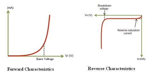
It generally shows the relation between bias voltage and current of a diode. The V-I characteristics of a diode can be forward or reverse. The graph showing the forward bias voltage and forward current is known as the forward characteristics, and that showing the reverse bias voltage and reverse current is known as the reverse characteristics.
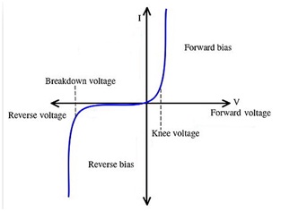
The forward characteristics of a diode is non linear. The forward current increases slowly in the beginning and shows a sudden rise at a certain value of forward voltage. This voltage is known as the threshold voltage or Knee voltage. This is because the resistance is very low in forward biased condition. The current in the reverse bias is due to the flow of minority carriers. The reverse current shows a sudden increase at a particular region. The corresponding voltage is termed as the reverse breakdown voltage.
• A p-n junction diode
• 3 V battery
• 50 V battery
• High resistance rheostat
• 0-3 V voltmeter
• 0-50 V voltmeter
• 0-100 mA ammeter
• 0-100 µA ammeter
• One way key
• Connecting wires
• Connections are made as per the connection diagram.
• Insert the key. Arrange the sliding contact of the rheostat to minimum.
• Now, gently move the rheostat contact to provide a positive bias voltage.
• Note the voltmeter and milli ammeter readings.
• Repeat the process by increasing the forward current in equal steps by changing the rheostat slider.
• It can be noted that, initially the current increase very slowly. For a certain value of voltage, it shows a sharp increase. The corresponding voltage represents the knee voltage of that diode.
• Plot a graph with forward voltage along X axis and forward current along Y axis. The graph shows the forward V-I characteristics of the given p-n junction diode.
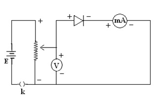
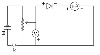
• Make the circuit diagram as shown in the figure.
• Insert the key. Arrange the sliding contact of the rheostat to maximum.
• Move the sliding contact of the rheostat to provide a reverse bias voltage.Note the voltmeter and micro ammeter readings.
• Note the voltmeter and micro ammeter readings.
• Repeat the process by changing the reverse voltage in equal steps.
• The current increases slowly in the beginning and then rapidly when the reverse voltage becomes a certain value. This voltage is known as the reverse breakdown voltage.
• Plot a graph with reverse voltage along X axis and reverse current along Y axis. The graph shows the reverse V-I characteristics of the given p-n junction diode.
The forward and reverse characteristics of the given p-n junction diode is drawn.
For the forward characteristics of the given p-n junction diode, a graph is plotted with forward voltage along X axis and forward current along Y axis. The forward current shows a sudden increase at certain forward voltage, which is known as the knee voltage.
For the reverse characteristics of the given p-n junction diode, a graph is plotted with reverse voltage along X axis and reverse current along Y axis. I t is noted that at a certain reverse voltage, the reverse current reaches its maximum level. Further increase in voltage does not increase this current. It is the reverse saturation current. However, with further increase in reverse voltage, the current shows a rapid rise at a certain value. It is known as the reverse breakdown voltage.
• http://epathshala.nic.in/wp-content/doc/book/flipbook/Class%20XII/12090-Physics%20Part-II/Chapter%2014/index.html
