

Updated on May 29, 2026
Ovonyx is developing a microelectronics memory technology called Ovonic Unified Memory (OUM). This technology is originally developed by Mr. Stanford Ovshinsky and exclusively licensed from Energy Conversion Devices (ECD) Inc. Ovonic unified memory -- its name is derived from ''Ovshinsky'' and ''electronic''.
OVM is also known as phase change memory because it uses unique thin-film phase change material to store information economically and with excellent solid-state memory properties. It would be the replacement of conventional memories like Magnetic Random Access Memory (MRAM), Ferro electric Random Access Memory (FeRAM or FRAM), Dynamic Random Access Memory (DRAM), and Static Random Access Memory (SRAM).
OVM allows the rewriting of CD & DVDs .CD & DVD drives read or write ovonic material with laser , but OVM uses electric current to change the phase of the material. The thin-film material is a phase-change chalcogenide alloy similar to the film used to store information on commercial CD-RW and DVD-RAM optical disks, based on proprietary technology originally developed by and exclusively licensed from Energy Conversion Devices.
Magnetic Random Access Memory (MRAM), a technology first developed in the 1970's, but rarely commercialized, has attracted by the backing of I.B.M. Motorola and others. MRAM stores information by flip flopping two layers of magnetic material in and out of alignment with an electric current. For reading and writing data, MRAM can be as fast as a few nanoseconds, or billionths of a second, best among the next three generation memory candidates. And if promises to integrate easily with the industry's existing chip manufacturing process. MRAM is built on top of silicon circuitry. The biggest problem with MRAM is a relatively small distance, difficult to detect, between it's ON and OFF states.
The second potential successor to flash, Ferro - electric Random Access Memory (FeRAM / FRAM), has actually been commercially available for nearly 15 years, has attracted by the backing of Fujitsu, Matsushita, I.B.M. and Ramtron. FRAM relies on the polarization of what amount to tiny magnets inside certain materials like perouikite, from basaltic rocks. FRAM memory cells do not wear out until they have been read or written to billions of times, while MRAM and OUM would require the addition of six to eight "masking" layers in the chip manufacturing process, just like Flash, FRAM might require as little as two extra layers.
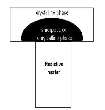
OUM is based on the information storage technology developed by Mr.Ovshinsky that allows rewriting of CD's and DVD's. While CD and DVD drives read and write ovonic material with lasers, OUM uses electric current to change the phase of memory cells. These cells are either in crystalline state, where electrical resistance is low or in amorphous state, where resistance is high. OUM can be read and write to trillionths of times making its use essentially nondestructive, unlike MRAM or FRAM. OUM's dynamic range, difference between the electrical resistance in the crystalline state and in the amorphous state - is wide enough to allow more than one set of ON and OFF values in a cell, dividing it into several bits and multiplying memory density by two, four potential even 16 times. OUM is not as fast as MRAM.
The OUM solid-state memory has cost advantages over conventional solid-state memories such as DRAM or Flash due to its thin-film nature, very small active storage media, and simple device structure. OUM requires fewer steps in an IC manufacturing process resulting in reduced cycle times, fewer defects, and greater manufacturing flexibility.
• Non volatile in nature
• High density ensures large storage of data within a small area
• Non destructive read:-ensures that the data is not corrupted during a read cycle.
• Uses very low voltage and power from a single source.
• Write/erase cycles of 10e12 are demonstrated
• Poly crystalline
• This technology offers the potential of easy addition of non volatile memory to a standard CMOS process.
• This is a highly scalable memory
• Low cost implementation is expected.
Under contract to the Space Vehicles Directorate of the Air Force Research Laboratory (AFRL), BAE SYSTEMS and Ovonyx began the current program in August of 2001 to integrate the chalcogenide-based memory element into a radiation-hardened CMOS process. The initial goal of this effort was to develop the processes necessary to connect the memory element to CMOS transistors and metal wiring, without degrading the operation of either the memory elements or the transistors. It also was desired to maximize the potential memory density of the technology by placing the memory element directly above the transistors and below the first level of metal
| Are you interested in this topic.Then mail to us immediately to get the full report.
email :- contactv2@gmail.com |
