


Updated on May 29, 2026
In the 21st century, the nanometer will very likely play a role similar to the one played by the micrometer in the 20th century The nanometer scale will presumably pervade the field of data storage. In magnetic storage today, there is no clear-cut way to achieve the nanometer scale in all three dimensions. The basis for storage in the 21st century might still be magnetism.
Within a few years, however, magnetic storage technology will arrive at a stage of its exciting and successful evolution at which fundamental changes are likely to occur when current storage technology hits the well-known superparamagnetic limit.
Several ideas have been proposed on how to overcome this limit. One such proposal involves the use of patterned magnetic media. Other proposals call for totally different media and techniques such as local probes or holographic methods. Similarly, consider Optical lithography. Although still the predominant technology, it will soon reach its fundamental limits and be replaced by a technology yet unknown. In general, if an existing technology reaches its limits in the course of its evolution and new alternatives are emerging in parallel, two things usually happen:
First, the existing and well-established technology will be explored further and everything possible done to push its limits to take maximum advantage of the considerable investments made. Then, when the possibilities for improvements have been exhausted, the technology may still survive for certain niche applications, but the emerging technology will take over, opening up new perspectives and new directions.
In recent years, AFM thermomechanical recording in polymer storage media has undergone extensive modifications mainly with respect to the integration of sensors and heaters designed to enhance simplicity and to increase data rate and storage density. Using these heater cantilevers, high storage density and data rates have been achieved. Let us now describe the storage operations in detail.
Thermomechanical writing is a combination of applying a local force by the cantilever/tip to the polymer layer, and softening it by local heating. Initially, the heat transfer from the tip to the polymer through the small contact area is very poor and improves as the contact area increases. This means the tip must be heated to a relatively high temperature (about 400oC) to initiate the softening. Once softening has commenced, the tip is pressed into the polymer, which increases the heat transfer to the polymer, increases the volume of softened polymer, and hence increases the bit size.
Our rough estimates indicate that at the beginning of the writing process only about 0.2% of the heating power is used in the very small contact zone (10-40 nm2) to soften the polymer locally, whereas about 80% is lost through the cantilever legs to the chip body and about 20% is radiated from the heater platform through the air gap to the medium/substrate. After softening has started and the contact area has increased, the heating power available for generating the indentations increases by at least ten times to become 2% or more of the total heating power.
With this highly nonlinear heat transfer mechanism it is very difficult to achieve small tip penetration and hence small bit sizes as well as to control and reproduce the thermomechanical writing process. This situation can be improved if the thermal conductivity of the substrate is increased, and if the depth of tip penetration is limited. These characteristics can be improved by the use of very thin polymer layers deposited on Si substrates as shown in figure 1.
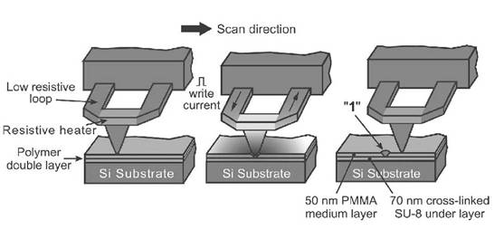
The hard Si substrate prevents the tip from penetrating farther than the film thickness, and it enables more rapid transport of heat away from the heated region, as Si is a much better conductor of heat than the polymer. By coating Si substrates with a 40-nm film of polymethylmethacrylate (PMMA) bit sizes ranging between 10 and 50 nm is achieved. However, this causes increased tip wear, probably caused by the contact between Si tip and Si substrate during writing. Therefore a 70-nm layer of cross linked photoresist (SU-8) was introduced between the Si substrate and the PMMA film to act as a softer penetration stop that avoids tip wear, but remains thermally stable.
Imaging and reading are done using a new thermomechanical sensing concept. The heater cantilever originally used only for writing was given the additional function of a thermal readback sensor by exploiting its temperature-dependent resistance. 'The resistance (R) increases nonlinearly with heating power/temperature from room temperature to a peak value of 500-7000oC. The peak temperature is determined by the doping concentration of the heater platform, which ranges from 1x10¹⁷ to 2x10¹⁸.Above the peak temperature, the resistance drops as the number of intrinsic carriers increases because of thermal excitation. For sensing, the resistor is operated at about 350oC, a temperature that is not high enough to soften the polymer as is the case for writing.
The principle of thermal sensing is based on the fact that the thermal conductance between the heater platform and the storage substrate changes according to the distance between them. The medium between a cantilever and the storage substrate -in our case air- transports heat from one side to the other. When the distance between heater and sample is reduced as the tip moves into a bit indentation, the heat transport through air will be more efficient, and the heater's temperature and hence its resistance will decrease. Thus, changes in temperature of the continuously heated resistor are monitored while the cantilever is scanned over data bits, providing a means of detecting the bits. Figure3 illustrates this concept.
| Are you interested in this topic.Then mail to us immediately to get the full report.
email :- contactv2@gmail.com |
