


Published on Nov 30, 2023
The measuring appliance amplifier is a double-end input differentiator amplifier, besides the high accuracy, the high stable characteristic, its output zero reference voltage may establish willfully through the REF base pin's voltage, this adjusted zero for us to float has provided the possibility.
The AD620 input end has reaches as high as 109O the input impedance; Input offset voltage 30uV, output offset voltage 400uV. The input bias current is very low, usually is highest in 0.5nA does not surpass 2nA; When the gain is 100, gain error 0.15%; Increases 100:00 syntype rejection ratios to reach as high as 130dB; Input noise 9nV/, output noise 72nV/. , The AD620 temperature stability also is very except for this outstanding:
The gain is bigger than 1:00, gain temperature coefficient for - 50ppm, input offset voltage and output offset voltage average temperature coefficient respectively be 0.3uV/ ? and 5.0uV/ ? .
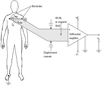
Fig: The AD620 finds its major usage in ECG systems
Here, we shall explore the internal working of the AD620 and try to emulate the characteristics of AD620.
1) We first note that the resistor R is the only passive element in this two-stage op-amp circuit: the function of R is biasing, i.e. setting up a constant dc bias current Ib. This current is then is replicated at various other locations for biasing other amplifier stages through current mirrors. In the op-amp circuit of Fig.6.3, the bias current Ib is the input current for the current mirror with two outputs: N0 and N1.
2) N2 and P2 combined together form current mirrors, distributing Ib to the rest circuit. Here, the input side of the mirror is N0 are the two outputs of the mirror. Since N3 and P3 are sharing the same gate-source voltage, the driver source N0 can replicate the bias current Ib as needed for biasing throughout the rest of the circuit. Different aspect ratios W/L of the mirror output transistors with respect to the input transistor can be used to scale the bias currents as needed (more about this in the quantitative analysis later)
3) N1 and N0 form the input differential pair, which is also the input of the first gain stage. P0 and P1 form the current mirrors for the differential pair N0 and N1. This bias current is provided by the voltage source Vdd, which acts as a DC current source.
4) M6 is the common source gain stage and it is also the second gain stage, note that the input of this gain stage is at node 1 which is the gate of P3, the output of this stage is at node 2 which is the drain of M6 and M6 is biased from node 1. The source of M6 is directly connected to the DC supply voltage VDD and hence no signal component.
