


Published on Nov 30, 2023
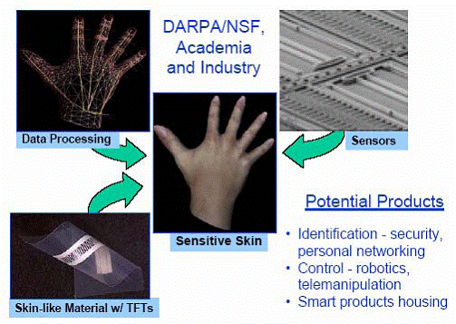
Sensitive skin is a large-area, flexible array of sensors with data processing capabilities, which can be used to cover the entire surface of a machine or even a part of a human body. Depending on the skin electronics, it endows its carrier with an ability to sense its surroundings via the skin's proximity, touch, pressure, temperature, chemical/biological, or other sensors.
Sensitive skin devices will make possible the use of unsupervised machines operating in unstructured, unpredictable surroundings among people, among many obstacles, outdoors on a crowded street, undersea, or on faraway planets. Sensitive skin will make machines "cautious" and thus friendly to their environment.
This will allow us to build machine helpers for the disabled and elderly, bring sensing to human prosthetics, and widen the scale of machines' use in service industry. With their ability to produce and process massive data flow, sensitive skin devices will make yet another advance in the information revolution. This paper surveys the state of the art and research issues that need to be resolved in order to make sensitive skin a reality.
- Sensitive Skin material will hold embedded sensors and related signal processing hardware. It needs to be flexible enough for attaching it to the outer surfaces of machines with moving parts and flexible joints.
- The skin must stretch, shrink, and wrinkle the way human skin does, or to have other compensating features. Otherwise, some machine parts may become "exposed" due to the machine's moving parts, and have no associated sensing.
- Wiring must keep its integrity when Sensitive Skin is stretched or wrinkled. This requirement calls for novel wire materials, e.g. conductive elastomers or vessels carrying conductive liquid, or novel ways of wire design with traditional materials, such as helical, stretchable wires
From the device point one might wish a Sensitive Skin to have some of the following capabilities:
. Flexible or deformable, Can be tiled or cut, This aspect ties in to cost and repair ability, High detectivity, On-skin switching and signal processing, Fault tolerances by distributing functions/computing, or protect processor units. Transmission by wire or optical fiber, or wireless: RF, UHF, free-space optical.
. Power by wire photovoltaics, RF, fuel cells, micro engines, or from energy harvesting - (skin-integrated mechanical power generators). Power storage in batteries. Or as fuel for fuel cells and micro engines.
. Sensitive Skin sensor components will be deployed in two dimensional arrays of sufficiently high density
. Smaller arrays may be of use as well: the key feature is that the skin should allow, by itself or with appropriate data processing, to identify with reasonable accuracy the points of the machine's body where the corresponding sensor readings take place.
. "Self-sensing" ability of the skin is highly desirable; this may include sensing of contamination, dust, chemical substances, temperature, radiation, as well as detection of failure of individual or multiple skin sensors and the ability to work around failed areas.
. The ability to measure distance to objects would be a great advantage for enabling dexterous motion of the machine that carries the skin
Sensitive Skin will be a form of large-area electronics, and a large-area electronics industry already does exist. Flat panel displays, including active matrix liquid crystal displays and plasma panel displays, are products of this industry. The medical X-ray sensor panels that are in pilot use likewise are large-area electronic products. These flat panel products use glass plates for substrate and encapsulation, and are rigid. Flexible, active circuit technology is just coming out of the research laboratory, like OLEDs on plastic foil, laser crystallized polysilicon on polyester, TFTs on polyamide, and OLEDs integrated with TFTs on steel foil. In other words, the basic technology for flexible skin electronics is coming together.
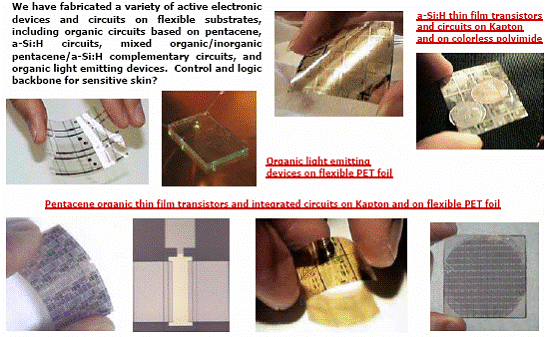
Organic thin film transistors (OTFT) are based on a new class of materials called conjugated polymers. Organic thin film transistors are considered as a competitive alternative to the traditional inorganic semiconductor based thin film transistors. In terms of performance, organic materials are not likely to catch the inorganic semiconductor based transistors, however, low cost, large area, and reel-to reel manufacturing can bring new opportunities where inorganic electronics cannot obtain.
The capability of plastic-based displays provides broad applications for industrial and product designers. The technical venture plans to create flexible organic-TFT technology, which has the potential to dramatically reduce the cost of display back planes while enabling the fabrication of lower cost flexible display devices.
Organic materials are poised as never before to transform the world of circuit and display technology. The future holds tremendous opportunity for the low cost and sometimes surprisingly high performance offered by organic electronic and optoelectronic devices. Using organic light-emitting devices (OLEDs), organic full-color displays may eventually replace liquid-crystal displays (LCDs). Such displays can be deposited on flexible plastic foils, eliminating the fragile and heavy glass substrates used in LCDs, and can emit bright light without the pronounced directionality inherent in LCD viewing, all with efficiencies higher than can be obtained with incandescent light bulbs.
The materials needed for the printing of sensor circuits include metallic conductors, insulators, semiconductors for transistors and light emitters, piezoelectric materials, etc. This approach to the printing of active circuits explores the territory that lies between IC’s and printed-wire boards. In effect, sensitive skin devices will contain active circuits monolithically integrated with their packaging. Completed thin-film circuits are at most a few micrometers thick. Therefore, the substrate and encapsulation constitute the bulk of the finished product. Reduction of their weight and thickness becomes important. When the substrate is reduced to a thickness where it becomes flexible, it also becomes usable in continuous, roll-to-roll paper-like production.
The finished circuit then is a flexible foil, and using equally thin encapsulation will preserve this flexibility. Rugged thin-film circuits are a natural consequence of the mechanics of thin foil substrates. In devising printing techniques for fabricating sensitive skin, the questions of feature size and of overlay registration must be answered. The development of microelectronics has shown that the search for high pattern density is one of the main drivers of IC technology. Therefore, it is instructive to estimate the density of active devices that could be produced by using conventional printing techniques.
The physical limits of several printing techniques are considerably finer than the resolution and registration of conventional printing equipment. Laser writing can produce a resolution of the order of 1 micro meter. Nanoimprinting has demonstrated a resolution in the tens of nanometer range. The density of directly printed devices can be raised orders of magnitude above ~ 10000 per square centimeter.
In order to fabricate novel devices that incorporate ink jet printed organic light emitting diodes and integrated active circuits based on printed organic logic components, it is highly desirable that all the other circuit components and connections can be printed with a compatible technology. These components and connections can include resistors, capacitors, diodes, inductors, sensors, transducers, and interconnects. Because the material properties and the material patterns are optimized best when done in separate steps, the application or modification of active material in IC fabrication is separated from its patterning. To directly print active circuits, one must devise materials that can be applied and patterned in a single step.
| Are you interested in this topic.Then mail to us immediately to get the full report.
email :- contactv2@gmail.com |
